Table of contents
Table of contents
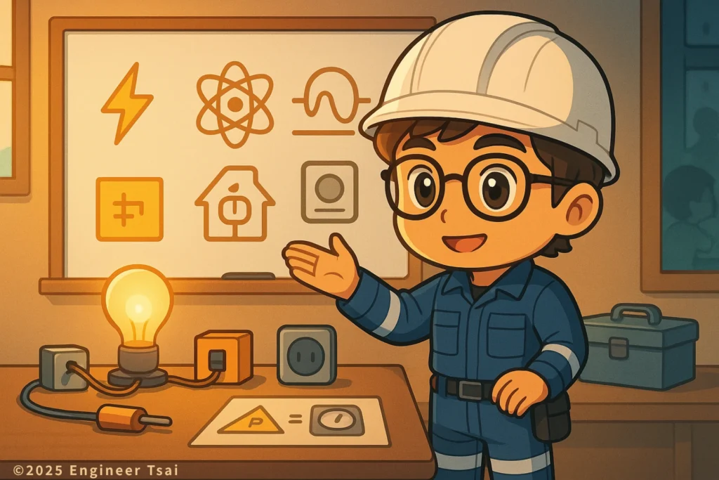
If you’re still building your foundation in basic electricity, start with this beginner-friendly overview: 🔹 “Electricity 101: The Complete Beginner’s Guide to How Power Really Works”
After reading it, the concepts in this article will make a lot more sense.
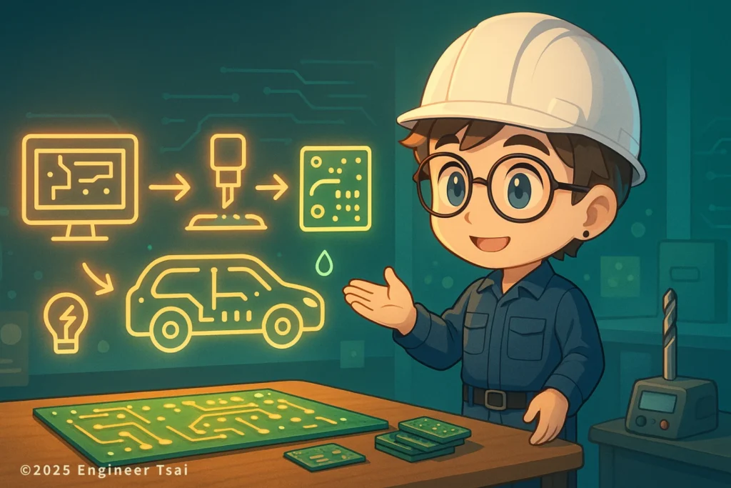
▶️ Watch: How PCBs are made — from a green panel to shipping
A lot of people see a PCB (printed circuit board) for the first time and think:
“It’s just a green board with some gold-ish traces and white text.”
This article breaks down the PCB manufacturing process step by step, so you’ll know what a board house is checking—and how to avoid common prototype rejections.
But the moment you walk into a real PCB fab, you realize something fast: the PCB manufacturing process is basically precision layer-by-layer construction—every layer has to line up, get pressed, drilled, and then the hole walls have to become conductive copper. After that, the board still needs protection, labels, surface finish, and testing before anyone dares to ship it.
If you’re learning circuit design, or you’ve already finished your schematic/PCB layout and you’re about to send it to a board house for prototyping, this article can save you real time and real money:
you’ll understand what the fab cares about, where projects usually fail, and how to design in a way that matches manufacturing reality.
Chapter 1 — What does the PCB manufacturing process really look like? A “day on the line” story
Let’s compress the whole PCB manufacturing process into one line first:
Design files (Gerber + drill files) → inner-layer imaging → lamination → drilling → plating to make hole walls conductive → outer-layer imaging → solder mask → silkscreen → surface finish (HASL / ENIG / OSP) → electrical test + visual inspection → routing/depaneling → shipping
Once you understand the PCB manufacturing process, DFM feedback from the board house will feel a lot less “random.”
It’s a long chain, but the mental model is simple: you “build each layer’s pattern,” press layers into one board (lamination), drill holes, turn those hole walls into copper conductors (plating), then protect and label the outside (solder mask + silkscreen + surface finish), and finally verify it before it leaves the factory.
And here’s the key reality check: a PCB isn’t “manufacturable” just because you can draw it. It’s closer to: “every trace and feature you draw has to be producible by real machines with real tolerances.” That’s why most board houses run DFM (Design for Manufacturability) checks first—especially on trace/space, minimum drill sizes, annular rings, solder mask openings, and anything that looks cool in CAD but becomes painful on the line.
Chapter 2 — How inner layers are made: imaging, developing, and etching is basically stencil work
If your PCB is multilayer (4-layer, 6-layer, and up), the inner layers are built first.
A common flow looks like this: start with copper-clad laminate, apply photoresist, “image” your inner-layer pattern with exposure, develop it so the protected areas remain, and then etch away the unwanted copper. What’s left is your inner-layer circuitry.
If you want a simple analogy, think stencil + paint removal:
you protect what you want to keep, then remove everything else, and the pattern appears.
This stage often includes AOI (automated optical inspection) to catch opens, shorts, nicks, and inconsistent line widths. Because once inner layers get laminated inside the board, fixing a mistake becomes “almost impossible”—so inner layers are where “inspect first, then move forward” really matters.
Chapter 3 — Why multilayer PCBs cost more: lamination + registration
The most labor-intensive (and risk-sensitive) part of multilayer boards is lamination.
The fab stacks inner-layer cores with prepreg (a fiberglass/resin bonding layer), adds outer copper foil, then uses heat and pressure to press the entire stack into one solid board.
Imagine building a layered sandwich where every layer has to line up. If a layer shifts, then drilling and outer-layer patterns won’t land where they’re supposed to. In PCB terms: bad registration means vias and pads won’t align, and that’s a fast way to scrap boards.
That’s why you’ll hear fabs talk about registration, thickness tolerance, and layer-to-layer misalignment. Materials expand with heat, resin flows under pressure, and the factory has to control all of it with process settings and experience.
Chapter 4 — Drilling and plating: vias are the 3D shortcuts of a circuit
After lamination, the board looks like a solid “layer cake.” Next comes drilling.
All the vias you see in layout—through-hole vias, plated through-holes (PTH), and even blind/buried vias—start here. The drill creates the hole, but right after drilling, the hole wall is mostly fiberglass and resin, so it’s not conductive yet.
That’s why the next critical step is plating.
The factory cleans and conditions the hole wall, deposits a thin “seed” copper layer (electroless copper), and then electroplates copper to build thickness—turning the hole wall into a conductive copper barrel.
Think of vias like elevators in a building:
traces are hallways on one floor; vias are how you travel between floors. Without vias, multilayer routing doesn’t exist.
Chapter 5 — Solder mask, silkscreen, and surface finish: green coating, white labels, gold fingers
Once the outer-layer copper is patterned, the board can technically conduct electricity—but it’s not ready for real life. Bare copper oxidizes, it’s easy to contaminate, and it’s easy to accidentally short things during assembly.
So the next “most visible” steps are usually these three:
Solder mask: the green layer isn’t decoration—it’s protection
Solder mask is the protective coating (green is most common, but red/black/blue/white exist too). It does two super practical things:
it prevents solder from bridging where it shouldn’t, and it reduces the risk of dust/moisture causing tiny leakage paths or micro-shorts.
Silkscreen: the white text is for humans, not for electricity
Silkscreen includes reference designators, polarity marks, orientation arrows, logos, and part labels. When you assemble or debug a board, you’ll be grateful it exists.
A board without silkscreen feels like troubleshooting in a packed stadium—everything is there, but finding the exact thing you need takes way longer than it should.
Surface finish: HASL vs ENIG vs OSP—what’s the difference?
Surface finish is mainly about: oxidation protection + reliable soldering + stable electrical contact.
Common options include HASL, ENIG, and OSP. Each comes with tradeoffs in cost, flatness, assembly compatibility, and long-term reliability. If you’re doing a simple prototype and hand soldering, the fab will often recommend the most common “easy to assemble” choice.
Chapter 6 — Testing, routing, depaneling, and shipping: boards aren’t done until they pass
The last stage is the one beginners often underestimate: the factory doesn’t just “finish the board” and hand it to you. It tests, inspects, and sorts.
Common checks include:
- Electrical test (E-test): confirms no shorts and no opens—at minimum, the netlist is electrically valid.
- Visual inspection: checks solder mask damage, copper scratches, silkscreen clarity, pad defects, and general workmanship.
- Routing / depaneling: uses a router or V-score/V-cut to separate the PCB from the larger manufacturing panel into the individual boards you actually hold.
So here’s the mindset shift: in CAD you see a “clean design.” In the fab, they see “how to build it, how to verify it, and how to ship it.” Once you understand that angle, you’ll naturally start designing with manufacturing margin instead of pushing everything to the limit.
That’s the real value of learning the PCB manufacturing process: you start designing layouts that survive real-world fabrication, not just CAD screenshots.
Wrap-up — Know the process, design a PCB that won’t get kicked back
At the end of the day, learning the PCB manufacturing process is really learning one honest rule:
every line you draw has to become something a machine can reliably produce.
Once you know how etching behaves, why lamination can shift layers, and how vias only work because plating turns hole walls into copper, you’ll stop creating layouts that are “theoretically fine” but “manufacturing nightmare.”
If you want, I can turn this into a practical “first-time PCB prototyping checklist” (DFM-style) you can run before you send files to a board house—so you avoid the most common reasons for rejected files and last-minute redesigns.
📌 Extended reading:
🔹“What is a PCB?” Understand its role in your circuit
If you’re still at the “what does a PCB actually do?” stage, read this first—then the manufacturing steps will click way faster.
🔹Basic parts of an electric circuit: source, conductor, and load
On a PCB, copper traces are conductors, pads are connection points, and components are loads. Get the core mental model right, and everything becomes easier to visualize.
🔹What is a short circuit? Why PCBs are so sensitive to it
Trace spacing, solder mask, cleanliness, and electrical testing are all basically “anti-short-circuit” strategies. This makes DFM rules feel much less arbitrary.
If you want a quick glossary from external sources, here are a few good starting points: Printed circuit board (PCB), Gerber format (official downloads), Solder mask, ENIG, HASL, and IPC printed board design standards.
PCB manufacturing FAQ
Q1: In the PCB manufacturing process, which step is most likely to cause problems?
A: The most common failure points are usually (1) trace/space pushed too tight (etching control gets hard), (2) lamination registration / thickness tolerance (especially on multilayer boards), and (3) hole wall quality + copper plating thickness (reliability). Beginners often get hit by this: a layout that looks clean in CAD but leaves no manufacturing margin, so DFM flags it and the board house asks for changes.
Q2: What’s the difference between single-sided, double-sided, and multilayer PCB manufacturing?
A: For single- vs double-sided boards, the big difference is whether you’re connecting both sides through plated holes and how precisely the two sides align. Multilayer boards add inner-layer fabrication plus lamination (stacking/pressing layers), which increases process steps, variables, and registration control—so cost usually rises a lot.
Q3: What are vias, blind vias, and buried vias?
A: A via is a conductive hole that connects different copper layers. A plated through-hole (PTH) connects top to bottom. A blind via connects an outer layer to an inner layer but doesn’t go all the way through. A buried via sits entirely inside the board and isn’t visible from the outside. Blind/buried vias often require extra lamination steps and/or laser drilling, so they typically increase lead time and price.
Q4: Why are most PCBs green? Can I choose black or white?
A: Green solder mask is the most common, most mature, and usually has stable yields. Black or white is absolutely possible, but color/reflectivity can affect optical inspection and visual yield, so some board houses may warn you about cost/lead-time differences—especially on small prototype runs.
Q5: HASL vs ENIG — which surface finish should I choose?
A: A simple rule of thumb: if you want cost-friendly and easy hand soldering, HASL is often enough. If you want flatter pads for fine-pitch parts and more consistent assembly (and you like the premium look), ENIG is commonly chosen for prototyping and production. The best choice still depends on component pitch, assembly method, reliability needs, and your board house’s recommendation.
Q6: For my first PCB prototype order, what files do I need to send?
A: Typically you’ll need Gerbers (copper layers, solder mask, silkscreen, outline), Excellon drill files, plus your specs: material, thickness, copper weight, solder mask color, and surface finish. If you need controlled impedance, a specific stackup, or blind/buried vias, state it up front to avoid back-and-forth and schedule slips.
—
Have you ever had a PCB come back and suddenly one area is impossible to solder—or it shorts way too easily?
Or you’ve been “kicked back” by a board house with a reason that felt confusing? Drop a comment and I’ll turn the most common rejection reasons into a practical “prototype DFM avoidance checklist.”
Read next in this topic
- What Is Electricity ? Everything You Need to Know
- Current & Voltage for DIY Enthusiasts : Unlock the Basics
- AC vs DC: What’s the Difference and Why It Matters (From Phone Charging to 120 V Home Power)
- Basic Parts of an Electric Circuit (Power Source, Wires, Loads)
- Conductor vs Insulator: How Your Home’s Wiring Keeps You from Getting Shocked
- Ohm’s Law Explained: V = IR for 120V Home Circuits
- What Is a Resistor? How It Works, Types, and How to Choose the Right One
- Series vs Parallel Circuits: Simple Guide for Home Wiring (With Formulas & Examples)
- How Electromagnetic Wave and Electricity Shape Modern Technology
- What Is Voltage? Simple Definition, Everyday Examples, and Safety Tips
- What Is a Battery? How It Works, Types, and Everyday Uses Explained
- What Is Ampere’s Law? A Visual Guide to How Current Creates Magnetic Fields
- What Does a Capacitor Do? Uses, Energy Storage, and Everyday Examples
- Types of Electrical Wire: How to Choose the Right One for Your Home
- How AC Power Is Converted to DC: What’s Really Inside Your Phone Charger?
- Electrical Energy Conversion: How Energy Transforms for Everyday Use
- Magnetic Field and Current: The Core Relationship Behind Motors, Generators, and Wireless Charging
- How Do Magnets Work? From Fridge Magnets to Maglev Trains
- What Is Inductance? Inductor Basics for Real-World Circuits
- What Is Impedance? A Plain-Language Guide to Resistance, Inductive Reactance, and Capacitive Reactance