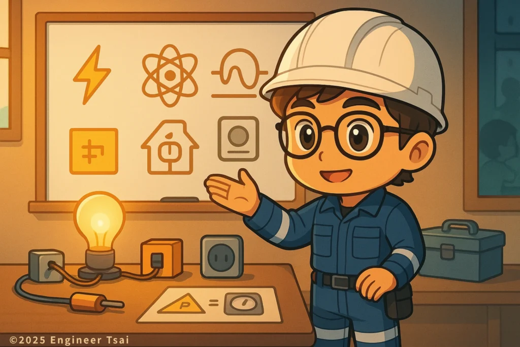
On this page
Table of contents
The PCB prototyping process is often misunderstood as “draw a schematic and send it to a factory.” But once you actually start building electronics projects, you quickly realize the hardest part usually happens before ordering the board: turning an idea into something you can design, manufacture, test, debug, and improve.
In this guide, we’ll use a simple door alarm project as a real-world example to walk through the complete PCB prototyping process: functional planning, EasyEDA schematic capture, ESP32-C3 control logic, MOSFET buzzer driving, magnetic switch input protection, PCB layout, and finally exporting Gerber, BOM, and CPL files for fabrication services such as JLCPCB.
This isn’t just an article about “making a buzzer beep.” The bigger goal is helping you understand how a real electronics project goes from an idea → a circuit → a manufactured PCB you can physically hold in your hand.
▶️ Watch now: How the PCB prototyping process turns an idea into a real PCB
This video demonstrates the complete PCB prototyping process using a door alarm project: breaking the design into modules, creating the schematic, planning PCB layout, exporting manufacturing files, and turning a digital design into a real circuit board.
If the video made you wonder things like “How do I turn my electronics idea into a PCB?”, “How do I start using EasyEDA?”, or “What’s the difference between Gerber, BOM, and CPL files?”, then this beginner-friendly guide to the PCB prototyping process is exactly where you should start.
Chapter 1 — PCB prototyping process: don’t rush into schematics before defining the functions
The most common beginner mistake in the PCB prototyping process usually isn’t “bad drawing skills.” It’s starting too fast.
A lot of people get excited about an idea, immediately open PCB software, start placing components and routing traces—then halfway through realize they never thought about basic system questions:
- Where does the power come from?
- Do I need status LEDs?
- Can the MCU drive the buzzer directly?
- Should I add test points?
- Will long external wires introduce noise?
- Do I need ESD protection?
A stable PCB prototyping process starts by asking a much more important question first:
What functional blocks does this device actually need?
A door alarm may sound simple—“the door opens and the alarm sounds.” But when you break it down, it’s actually a small embedded system. It needs power management, input sensing, a control core, and output devices such as buzzers or LEDs.
This step matters because once the functions are clearly separated, the rest of the PCB prototyping process becomes easier: component selection, schematic design, PCB layout, debugging, and future revisions all become more structured.
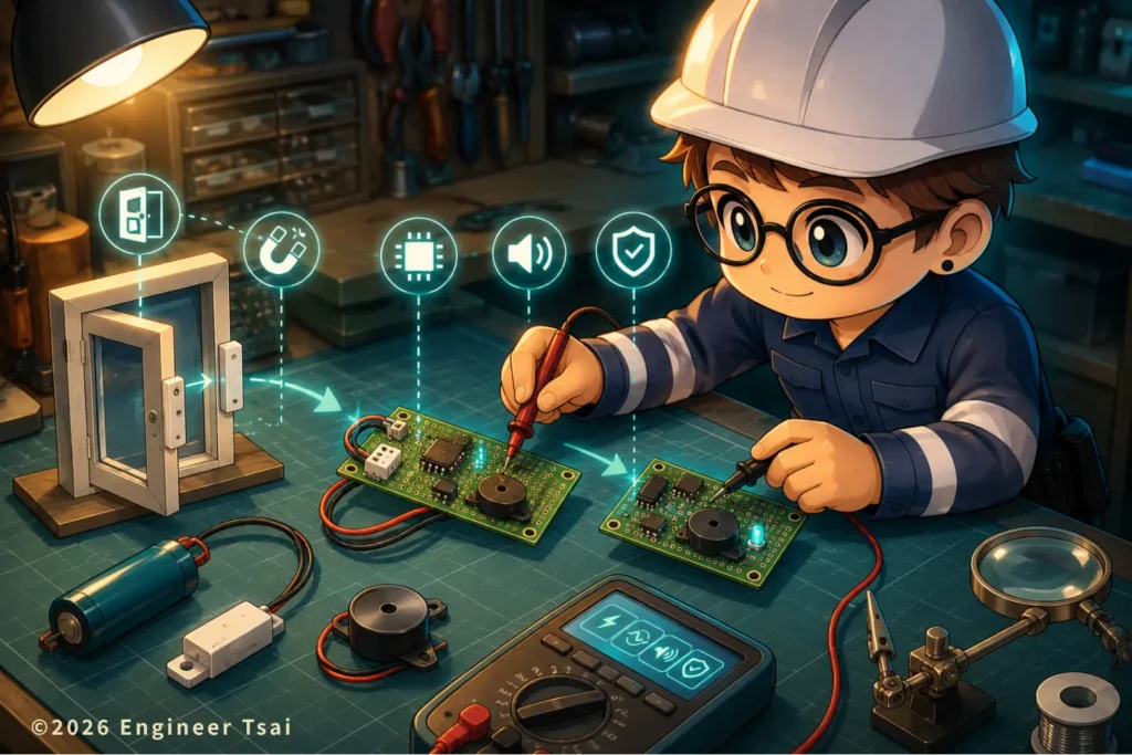
Chapter 2 — Breaking a door alarm into modules: power, input, control, and output
This door alarm project can be divided into four major modules.
The first module is power. You need to decide how the board will be powered. Battery? USB? External DC supply? If the control core runs on 3.3V, then you’ll need voltage regulation to provide a stable rail. Power isn’t something you “add later”—it’s the foundation of the entire PCB.
The second module is input sensing. A common door alarm input is a magnetic reed switch. When the door is closed, the magnet stays near the sensor. Once the door opens, the switch state changes and the MCU detects the event.
The third module is the control core. For a basic alarm, simple logic might work. But if you eventually want BLE, smartphone notifications, low-power modes, or IoT connectivity, using something like an ESP32-C3 gives you much more room to grow.
The fourth module is output. The obvious choice is a buzzer that sounds when the door opens. You may also want LEDs for debugging and status indication. Even these “simple” outputs require real design decisions involving GPIO limits, drive current, startup behavior, and switching noise.
Once you divide the project into these four blocks—power, input, control, and output—the PCB prototyping process starts feeling much more like engineering and much less like randomly drawing wires.
Chapter 3 — EasyEDA schematic design: turning functional blocks into a real circuit
After defining the functions, the next stage in the PCB prototyping process is schematic design.
For this project, EasyEDA is a great beginner-friendly option because it supports the entire workflow: schematic capture, PCB layout, and manufacturing file export in one ecosystem.
A practical approach is designing the schematic block-by-block instead of drawing everything at once.
For example, the output section is usually the easiest place to start. When the door opens, you want the LED to turn on and the buzzer to sound.
The LED cannot connect directly to power, so it needs a current-limiting resistor. In a 3.3V system, 1kΩ is a safe and beginner-friendly choice that avoids excessive current while still giving visible brightness.
The buzzer requires more planning. Many beginners try connecting a buzzer directly to an MCU GPIO pin, but GPIO current capability is limited, and buzzers can introduce noise or transient loads.
A more reliable approach is letting the MCU control a MOSFET, while the MOSFET switches the actual buzzer current.
This teaches one of the most important lessons in the PCB prototyping process:
The MCU gives commands. The driver handles the power.
The same concept later applies to relays, motors, LED strips, pumps, and many other loads.
Chapter 4 — Design details: why MOSFETs, filtering, and ESD protection matter
A lot of beginners focus only on one thing during PCB prototyping: “Does the circuit work?” But a reliable board isn’t just about whether it powers on. You also need to think about false triggering, electrical noise, static discharge, and whether long external wires might inject spikes directly into the MCU.
Let’s start with the MOSFET. In this project, the buzzer is controlled using an N-channel MOSFET as a low-side switch. The positive side of the buzzer connects to power, while the negative side connects through the MOSFET. When the MCU drives the Gate high, the MOSFET turns on and the buzzer sounds.
But the Gate shouldn’t just be wired directly without thinking. MOSFET gates behave capacitively, meaning they charge and discharge during switching. That’s why designers often add a small gate resistor—something like 100Ω—to soften the switching edge and reduce ringing, spikes, and noise.
The Gate also shouldn’t be left floating. During MCU startup, GPIO pins may not yet be initialized, and without a defined default state, the buzzer could randomly chirp during boot. A common fix is adding a 100kΩ pull-down resistor so the MOSFET stays OFF until the MCU intentionally turns it on.
Now look at the door sensor input. Magnetic reed switches are often mounted on doors or windows, which means the wires can become relatively long. Long wires can act like antennas, bringing noise, static electricity, or surge spikes into the board.
That’s why the input usually needs proper pull-up or pull-down resistors so the MCU always sees a stable logic level. You might also add a small resistor like 220Ω for protection, combined with a 100nF capacitor for filtering. This helps suppress switch bounce and high-frequency noise.
If you want a more robust design, the external connector area can also include ESD protection so static discharge or sudden spikes don’t hit the MCU pins directly. These parts may look small and unimportant, but they’re often the difference between a board that merely “works” and one that feels stable and durable in the real world.
Chapter 5 — PCB prototyping process layout tips for beginners
Once the schematic is finished, the next step is PCB layout. This is where many beginners get nervous, because layout feels much more “real” than schematic design. The board layout directly affects whether you can solder it, assemble it, test it, or troubleshoot it later.
Rule #1: Place components based on real-world usage. Door sensor terminals usually belong near the edge of the PCB because external wires need to enter the board. Should the LED be visible through the enclosure? Should the buzzer face outward? Will the USB connector hit the case wall? These mechanical considerations should already be part of your layout thinking.
Rule #2: Keep power flow easy to understand. Power is the backbone of the entire board. If your regulator, capacitors, MCU, and loads are connected through messy routing, debugging later becomes painful. Beginners don’t need perfect professional-level power design immediately, but at minimum the power entry, regulator section, and 3.3V distribution path should feel logical and organized.
Rule #3: Keep noisy areas away from sensitive signals. Buzzers, power switching circuits, and long external wires can introduce noise. Even if this isn’t a high-speed board, it’s still good practice to mentally separate input, output, and power sections.
Rule #4: Don’t shrink the first revision too aggressively. Many beginners try to make their first PCB as tiny as possible. The result is cramped routing, poor spacing, no room for test points, and difficult soldering. For your first revision, the priority isn’t beauty—it’s whether the board can be manufactured, soldered, tested, and modified.
Many PCBs also use a GND copper pour (ground plane) to improve grounding continuity and reduce certain types of noise. As a beginner, you don’t need to fully master high-speed layout or impedance control immediately, but you should start building the habit of keeping power routing clear and ground return paths solid.
This is one of the most important ideas in the PCB prototyping process: your first PCB revision is not the finish line—it’s the starting point for discovering problems.
Chapter 6 — What to prepare before sending your PCB to manufacturing: Gerber, BOM, CPL, and PCBA explained
Once your PCB layout is finished, the next step is sending the design to a manufacturer. This is where you’ll encounter several common terms: Gerber, BOM, and CPL.
Gerber files are essentially the manufacturing drawings that PCB factories understand. They describe the copper layers, solder mask, silkscreen text, drill holes, and overall board structure. If you’re only ordering bare PCBs, Gerber files are the most essential output.
BOM stands for Bill of Materials. It lists all the components required for the board, including part numbers, quantities, package types, and reference designators. If you want the factory to assemble components for you (PCBA), the BOM becomes mandatory.
CPL stands for Component Placement List, sometimes called a Pick-and-Place file. It tells the assembly machine exactly where each component should be placed and what orientation it should have. In simple terms: the BOM tells the factory what parts to use, while the CPL tells them where those parts go.
If you don’t want to solder everything yourself, you can order PCBA directly. PCB refers to the bare board, while PCBA means the factory also places and solders the components for you. For beginners, PCBA can save huge amounts of hand-soldering time—but only if your BOM, CPL, footprints, and component orientations are all correct.
In the video, I used EasyEDA together with JLCPCB. One reason beginners like this workflow is that the manufacturing pipeline feels approachable: schematic → layout → Gerber export → upload → manufacturing. It makes the jump from “breadboard project” to “real PCB” feel much less intimidating.
Chapter 7 — Don’t rush to power it on: PCB testing is part of the real workflow
When people receive their first PCB, the instinct is usually: “Power it on immediately and see if it works.” But the safer and more professional approach is actually the opposite: don’t rush to apply power yet.
The first step is visual inspection. Does the PCB edge look clean? Are the pads intact? Is the silkscreen readable? If this is a fully assembled PCBA, double-check component orientation—especially ICs, diodes, electrolytic capacitors, connectors, and polarized parts.
The second step is checking the power rails. Before applying power, verify there’s no short between the power rail and GND. When you finally power the board, don’t immediately connect every load. First confirm the input voltage and verify the regulator is producing a stable 3.3V output.
Only after that should you move to functional testing. For this door/window alarm project, that means checking whether the reed switch input is detected correctly, whether the LED lights up, whether the buzzer sounds, and whether the system reacts properly when the door opens or closes.
If your first revision works perfectly, that’s amazing. But even if it doesn’t, that’s completely normal in hardware development. The first revision helps you discover mistakes. The second revision fixes those problems. By the third revision, the project slowly becomes the product you originally imagined.
That’s why the real PCB prototyping workflow isn’t just “make a board.” It’s: build it, test it, find problems, improve the design, and iterate. That iterative loop is what turns a small electronics experiment into something closer to a real product.
FAQ — PCB prototyping workflow and beginner PCB design questions
Q1: What is the difference between PCB and PCBA?
A: PCB refers to the bare printed circuit board itself. PCBA means the board has already been assembled with components. In other words, PCB is the empty board, while PCBA is the finished assembled circuit.
Q2: Is EasyEDA good for beginners?
A: Yes. EasyEDA is one of the most beginner-friendly PCB design tools because it combines schematic capture, PCB layout, and Gerber export in a relatively simple workflow. It also integrates easily with manufacturing services like JLCPCB.
Q3: What are Gerber files used for?
A: Gerber files are the manufacturing files used by PCB factories. They describe copper layers, solder mask, silkscreen, drill holes, and other board details needed for fabrication.
Q4: Why does my PCB work on a breadboard but fail after manufacturing?
A: Common reasons include incorrect footprints, missing pull-up/pull-down resistors, poor grounding, noisy routing, wrong connector orientation, or power integrity problems. Breadboards are forgiving in some ways, but real PCBs expose design mistakes more clearly.
Q5: Do beginners need to care about grounding and routing?
A: Absolutely. Even for simple projects, grounding and routing affect stability and reliability. You don’t need advanced high-speed design knowledge immediately, but you should already build good habits like short power paths, clean grounding, and sensible component placement.
Q6: Is it better to solder PCBs by hand or order PCBA assembly?
A: It depends on your goal. Hand soldering is great for learning and debugging. PCBA assembly saves time and improves consistency, especially for SMD parts or larger batches. Many beginners start with hand assembly, then move to PCBA once the design is stable.
Q7: What is the biggest mistake beginners make during the PCB prototyping process?
A: The biggest beginner mistake is rushing directly into PCB layout before fully defining the system functions, power flow, grounding, and testing strategy. A stable PCB prototyping process starts with clear functional planning, not just drawing traces.
📌 Recommended reading
🔹PCB Design for Beginners: 4 Steps to Design Your First PCB
This is the closest follow-up to this article. After you understand the PCB prototyping process, this guide helps you move into actual PCB design, layout thinking, and beginner-friendly design decisions.
🔹PCB Manufacturing Process in 12 Steps: How PCBs Are Made
This article explains what happens after you export Gerber files and send your board to fabrication, making it a strong next read after learning the prototyping workflow.
🔹What Is a Resistor? How It Works, Types, and How to Choose the Right One
Resistors appear throughout PCB design: current limiting, pull-up resistors, pull-down resistors, filtering, and signal protection. This guide helps beginners understand why they matter.
🔹What Does a Capacitor Do? Uses, Energy Storage, and Everyday Examples
Capacitors are essential for power stability, filtering, and noise reduction in PCB projects. This article gives beginners a clearer mental model before designing real boards.
🔹What Is a Transistor? How Small Currents Control Big Currents
This is useful background for understanding electronic switching. If your PCB uses drivers, buzzers, relays, or MOSFET-style switching logic, this article builds the foundation.
🔹What Is Electrical Grounding? A Simple Guide to Safer Power at Home
Grounding affects circuit stability, safety, noise behavior, and real-world reliability. This is a helpful supporting article for beginners learning why ground design matters.
References
- EasyEDA — Online PCB design and schematic capture platform
- JLCPCB — PCB fabrication and PCBA assembly services
- KiCad — Open-source PCB design software
- IEC (International Electrotechnical Commission) — International standards related to electronics and PCB design
If you want, leave a comment and tell me what kind of PCB you want to build first: a simple sensor board, smart home project, power electronics, automation controller, or something completely different. I can help you break down the workflow, common mistakes, and the easiest way to move from “idea” to your first real manufactured PCB.
I can also help you simplify the PCB prototyping process for your first project so you avoid the most common beginner mistakes.
Read next in this topic
- What Is Electricity ? Everything You Need to Know
- Current & Voltage for DIY Enthusiasts : Unlock the Basics
- AC vs DC: What’s the Difference and Why It Matters (From Phone Charging to 120 V Home Power)
- Basic Parts of an Electric Circuit (Power Source, Wires, Loads)
- Conductor vs Insulator: How Your Home’s Wiring Keeps You from Getting Shocked
- Ohm’s Law Explained: V = IR for 120V Home Circuits
- What Is a Resistor? How It Works, Types, and How to Choose the Right One
- Series vs Parallel Circuits: Simple Guide for Home Wiring (With Formulas & Examples)
- How Electromagnetic Wave and Electricity Shape Modern Technology
- What Is Voltage? Simple Definition, Everyday Examples, and Safety Tips
- What Is a Battery? How It Works, Types, and Everyday Uses Explained
- What Is Ampere’s Law? A Visual Guide to How Current Creates Magnetic Fields
- What Does a Capacitor Do? Uses, Energy Storage, and Everyday Examples
- Types of Electrical Wire: How to Choose the Right One for Your Home
- How AC Power Is Converted to DC: What’s Really Inside Your Phone Charger?
- Electrical Energy Conversion: How Energy Transforms for Everyday Use
- Magnetic Field and Current: The Core Relationship Behind Motors, Generators, and Wireless Charging
- How Do Magnets Work? From Fridge Magnets to Maglev Trains
- What Is Inductance? Inductor Basics for Real-World Circuits
- What Is Impedance? A Plain-Language Guide to Resistance, Inductive Reactance, and Capacitive Reactance